DNA translocation through nanopore
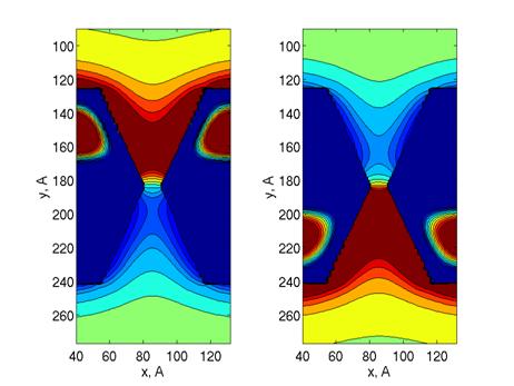
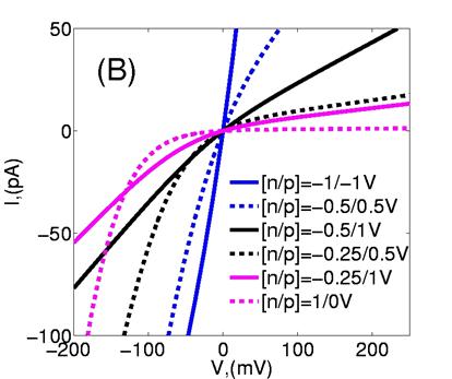
1. Protein and Ion Filter
We
shown recently that a semiconductor membrane made of two thin layers
of opposite (n-
and p-)
doping can perform electrically tunable ion current rectification and
filtering in a nanopore. Our model is based on the solution of the 3D
Poisson equation for the electrostatic potential in a double-cone
nanopore combined with a transport model. It predicts that, for
appropriate biasing of the membrane-electrolyte system, transitions
from ohmic behavior to sharp rectification with vanishing leakage
current are achievable. Furthermore, ion current rectifying and
filtering regimes of the nanopore correspond to different charge
states in the p-n membrane, which can be tuned with appropriate
biasing of the n-
and p-
layers.
Reference: "p-n semiconductor membrane for electrically tunable ion current rectification and filtering", M.E. Gracheva, J. Vidal and J.-P. Leburton, NanoLetters 7(6), p. 1717-1722 (2007). PDF (This article was featured in: www.physorg.com, www.nsf.gov, IOP, Beckman Institute, NCSA, Electrical and computer engineering Department of UIUC and around the world)
2. DNA Characterization with a Semiconductor Nanopore Membrane
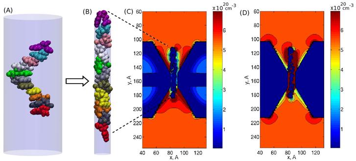
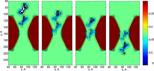
We evaluate the magnitude of the electrical signals produced by DNA translocation through a 1 nm diameter nanopore in a capacitor membrane with a numerical multi-scale approach, and assess the possibility of resolving individual nucleotides as well as their types in the absence of conformational disorder. We show that the maximum recorded voltage caused by the DNA translocation is about 35 mV, while the maximum voltage signal due to the DNA backbone is about 30 mV, and the maximum voltage of a DNA base is about 8 mV. Signals from individual nucleotides can be identified in the recorded voltage traces, suggesting a 1 nm diameter pore in a capacitor can be used to accurately count the number of nucleotides in a DNA strand. Furthermore, we study the effect of a single base substitution on the voltage trace, and calculate the differences among the voltage traces due to a single base mutation for the sequences C3AC7, C3CC7, C3GC7 and C3TC7. The calculated voltage differences are in the 5-10 mV range. The calculated maximum voltage caused by the translocation of individual bases varies from 2 to 9 mV, which is experimentally detectable.
Reference: ''Electrical Signatures of Single-Stranded DNA with Single Base Mutations in a Nanopore Capacitor'', M.E. Gracheva, A. Aksimentiev and J.-P. Leburton, Nanotechnology 17(13), p. 3160-3165 (2006). PDF (Journal cover paper)
3. Simulation of the electric response of DNA translocation through a semiconductor nanopore-capacitor
We propose a multi-scale/multi-material computational model for simulation of the electric signal detected on the electrodes of a metal-oxide-semiconductor (MOS) capacitor forming a nanoscale artificial membrane, and containing a nanopore with translocating DNA. The multi-scale approach is based on the incorporation of a molecular dynamics description of a translocating DNA molecule in the nanopore within a three-dimensional Poisson equation self-consistent scheme involving electrolytic and semiconductor charges for the electrostatic potential calculation. The voltage signal obtained from the simulation supports the possibility for single nucleotide resolution with a nanopore device. The electric signal predicted on the capacitor electrodes complements ongoing experiments exploring the use of nanopores in a MOS capacitor membrane for DNA sequencing.
Reference: "Simulation of the electric response of DNA translocation through a semiconductor nanopore-capacitor", M.E. Gracheva, A. Xiong, A. Aksimentiev, K. Schulten, G. Timp and J.-P. Leburton, Nanotechnology 17(3), p. 622-633 (2006). PDF (Highly accessed paper - top 10% of Institute of Physics (IOP) Publishing)
Other related papers
"Multilayered semiconductor membranes for nanopore ionic conductance modulation", M.E. Gracheva, D.V. Melnikov and J.-P. Leburton, ACS Nano 2(11), p. 2349-2355 (2008). PDF
"Simulation of electrically tunable semiconductor nanopores for ion current/single bio-molecule manipulation", M.E. Gracheva, J.-P. Leburton, J. Comput. Electronics 7(1), p. 6-9 (2008). PDF
"Electrolytic charge inversion at the liquid-solid interface in a nanopore in a doped semiconductor membrane", M.E. Gracheva and J.-P. Leburton, Nanotechnology 18, p. 145704-145710 (2007). PDF
"Electrically Tunable Solid-State Silicon Nanopore Ion Filter", J. Vidal, M.E. Gracheva and J.-P. Leburton, Nanoscale Research Letters 2, p. 61-68 (2007). PDF
Maria Gracheva's homepage, Physics Department, Clarkson University
Write me to gracheva@clarkson.edu
First created: Fri Aug 3 EDT 2001, last modified Thurs October 9 EDT 2008.